
Eeng.Content @Eeng.Content_2475
What is The OR GATE?
The OR gate is one of the basic logic Gates. It consists of at least two input terminals and one output terminal. It can have more than two inputs as well. The figure below shows a two-input OR gate.

Terminals A and B represent the inputs, and terminal F represents the output. The OR gate performs addition operations. The function of the OR gate is represented as follows:
--> F = A + B
The output values of the OR gate vary depending on the applied input values. All possible combinations of input and output values can be observed in the truth table provided below.
TRUTH TABLE:

From the truth table, it can be seen that when both input values are 0, the output value is 0. In all other cases, when at least one of the inputs is 1, the output is 1.
In addition, an OR gate can be simulated using the Logisim simulation program. By providing appropriate input and output values, the results can be observed. The following figures show the OR gate created using the Logisim program. Each figure shows four different cases given in the truth table.


The OR gate can also be created using combinations of transistors and resistors. Furthermore, the internal components that make up an OR gate circuit are as follows:
- Resistors
- BJT Transistors
- Power Supply
The internal structure of an OR gate is illustrated in the provided figure.
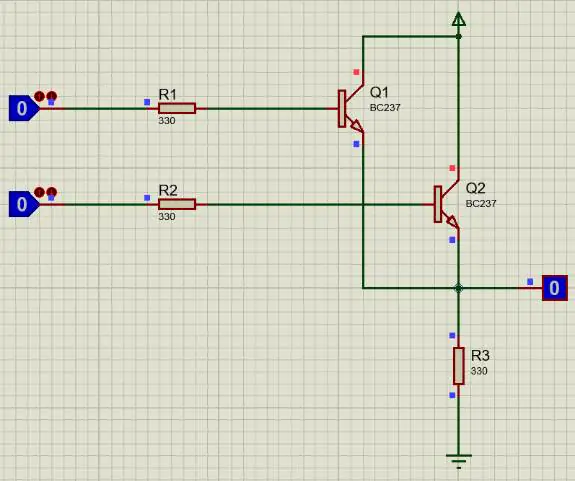
The transistors Q1 and Q2 shown in the circuit are in the cut-off state when both input values are logic 0. In other words, when both input values are logic 0, the transistors do not trigger. Therefore, no current passes through resistor R3, and the output is observed as 0. When at least one input value is logic 1, the transistor corresponding to the logic 1 input enters the conduction state. Once one of the transistors is triggered, current flows through resistor R3 and the output value is observed as logic 1.
Additionally, an electrical circuit can be constructed to achieve the function of an OR gate. The required components for this are:
- Buttons
- Voltage source
- Lamp
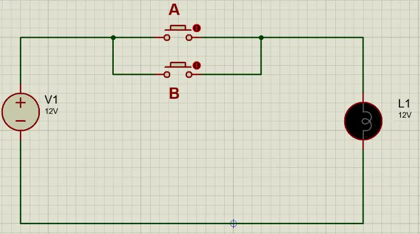
The circuit is shown in the provided figure. The buttons labeled A and B represent the inputs, while the lamp labeled L1 represents the output. The voltage source used in the circuit is 12 volts. The buttons are connected in parallel. To have the lamp lit, it is sufficient for only one of the buttons to be closed.
To put it more clearly, it represents logic 1 when the buttons are closed. If it is on, it represents logic 0. From the function of the OR gate, we know that when only one of the inputs is in the logic 1 state, the output is observed as logic 1. Similarly, in this circuit, when one of the buttons is in the off position (that is, in the logic 1 position), the lamp turns on (it gives the logic 1) value.
The OR internal structure and OR switching representation is given above were created using the Proteus simulation program.
---> The NOT GATE will be explained in detail in the next article.
1
No comments yet.